SiC Technology is Powering our Series 10000 Power Supplies – Here is Why
December 13, 2022 | Topics: EV Battery, Power Supplies, Sustainable Energy
Efforts to reduce the rate of climate change have resulted in advances in non-fossil fuel, renewable energy solutions and an accelerating rate of electrification in the transportation market. These new technologies are advancing the field of power supplies because of their high power requirements. Electric vehicles (EVs) can have battery packs sized in excess of 900 VDC with 95 kWh capacity. Fast EV charging systems have power ratings over 240 kW. The cell stacks of Hydrogen fuel cells, another developing technology for powering vehicles, can contain over 500 kW and can deliver up to 1000 A.
In contrast to the need to move away from fossil fuels, worldwide energy consumption is increasing. Server farms are one example of higher energy demand. To enable renewable energy to support them, server farms are transitioning from AC to DC distribution with operating voltages at 360 VDC and current capacity of 2000 A. Furthermore, new emerging technologies are using voltages in the 1800 VDC range.
Ready to Get Started? Request a Quote
The challenge of meeting market demand
In response to the market requirements for testing these higher power products, EA needed to develop higher output power supplies with higher output voltage, smaller test system volume, and lower cost/kW. Therefore, EA established the following goals for its new 10000-series programmable power supplies:
- Improved efficiency over existing programmable power supplies
- Increased DC output voltage to 2000 V
- Increased power density for reduced volume
- Reduced $/W cost.
The EA design team considered whether to use silicon (Si)-based transistor technology or use newer silicon carbide (SiC) power transistors. Using the existing Si semiconductor technology, power instrumentation can achieve a maximum efficiency of 93% when using a switch mode design that can operate at 40 kHz. If the power instrument uses a 5 kW power module, the achievable power density is 9.2 W/in3.
Limitations of a Si transistor-based power supply
A Si-based MOSFET (metal–oxide–semiconductor field-effect transistor) design needs three switching transistors to generate 5 kW. With a de-rating requirement for the MOSFETs of 30%, a 5 kW power module must use three 500 VDC modules in series to achieve 1500 VDC. Three of the 5 kW power modules can make up a 15 kW instrument. To meet a load demand of 150 kW, test system designers would need ten 15 kW power supplies. That quantity of supplies can fill a 42U high, 19-inch test rack. If the load demand were 450 kW, the test system would require three test racks consuming 18 sq ft of rack space. If the supplies were to operate at their maximum efficiency of 93%, the test system would generate a huge 31.5 kW of heat that would need to be removed.
Facing the challenges of meeting the goals for the new power supply family, the EA design team decided to go with SiC power transistors. The following paragraphs describe the benefits of SiC technology over the SiC alternative.
Higher efficiency of SiC MOSFETs over Si IGBTs
Prior generations of three-phase system-based power products utilized Si-insulated gate bipolar transistors (IGBTs). IGBTs have the capacity to support 1200 V and supply high current. However, IGBT conduction and switching losses are high. In contrast, SiC MOSFETs high-power semiconductors have much lower conduction and switching losses. As shown in Figure 1, SiC MOSFETs have a lower voltage drop than an equivalent IGBT when used as a switch. The RDS(on), the channel resistance of a saturated SiC MOSFET, is lower, particularly, at low loads, than the pn junction resistance of a saturated IGBT. Thus the conduction loss of an SIC MOSFET is lower than the IGBT’s conduction loss. The switching loss difference, as shown on the right side of Figure 1, is much more significant. The Si IGBT has a higher capacitance than the SiC MOSFET, and it takes the IGBT more time to switch off. Figure 1 indicates that a SiC MOSFET reduces the switching energy loss by a factor of 10.
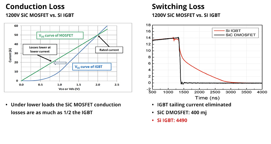
Figure 1. Switching and conduction loss comparisons between a SiC MOSFET and a Si IGBT
Higher switching speeds of SiC transistors compared with Si transistors
Since SiC MOSFETs take less time to switch, these transistors can operate at faster switching speeds. Figure 2 shows that a SiC MOSFET has a dv/dt rate almost twice the rate of a Si MOSFET for both turn-on and turn-off.
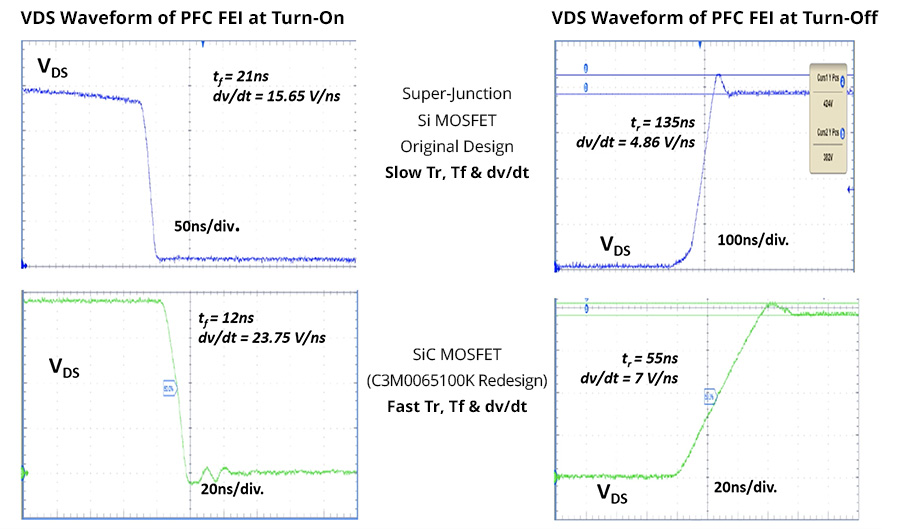
Figure 2. Turn-on and turn-off rates of a Si MOSFET (top plots) versus a SiC MOSFET (bottom plots)
Enhanced Reliability of SiC transistors
From a reliability standpoint, SiC MOSFETs have a higher breakdown voltage than their datasheet specification (see Figure 3). The breakdown margin of the SiC MOSFET demonstrates how robust the component is to transient over-voltages. At low temperatures, SiC MOSFETs have a specified breakdown voltage. IGBT manufacturers do not guarantee breakdown voltages at low negative temperatures. For example, a 1200 V IGBT is not capable of supporting 1200 V at -30° C. The device must be de-rated at that temperature.
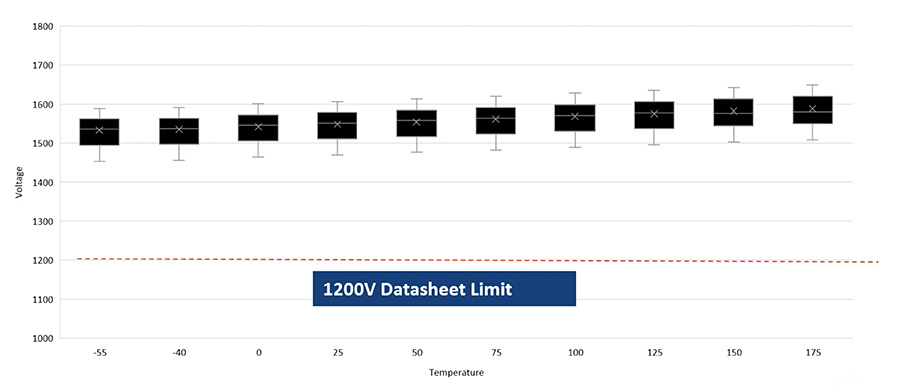
Figure 3. Actual breakdown voltage versus temperature of a SiC MOSFET. The plot represents measurements on sets of 15 components from three different production runs.
Reduced space consumption of SiC transistors
One more significant difference between SiC and Si power semiconductors is the die size. First, a SiC die is smaller than an equivalent power Si transistor die. Second, a Si transistor needs a back-biased diode to allow bi-directional current flow between the collector and emitter. The SiC transistor source-drain channel can conduct current in either direction. In addition, the SiC transistor has a parasitic body diode as part of the transistor structure. Thus the extra diode required for the Si transistor is not required for the SiC transistor. Using an example of a 1200 V transistor, the SiC transistor die area is about ¼ the die area of the Si transistor. Hence SiC component layouts in power circuits can exhibit lower stray inductance. Overall, the smaller SiC packages enable a higher power density in the end product.
Aggressive goals achieved in the new 10000-series power supplies
EA took advantage of SiC technology to develop a 30 kW programable power supply in a 4U high enclosure with models that can output 2000 V. The benefits as compared with Si-transistor-based models:
- Improved efficiency by 3%
- Increased power density by 37%
- Reduced floor space of a 240 W power supply system by 33%
- Reduced heat generation of a 240 W power supply system by 42%
- Reduced $/W by 15 – 20%.
Taking advantage of higher speed switching with SiC transistors, the new 10000-series switch mode AC-DC converters operate at approximately 60 kHz. That is 30% faster than the DC-DC converters of other manufacturers’ power supplies which switch at around 30 – 40 kHz. The 10000 series higher switching frequency enabled reduction in both the size of magnetic components and the size of the amplifiers. Not only did the magnetic components shrink by 30% in mass, but the design required one less inductive component saving valuable space and generating less heat.
Get more information
For more complete details on SiC power MOSFETS vs Si transistors, see our white paper, The Benefits of Using SiC Technology in Next Generation Programmable Power Supplies, an036_benefits-of-using-sic_en.pdf (elektroautomatik.com). Also, watch our on-demand webinar on the same subject, Webinars – EA Elektro-Automatik (eapowered.com).